

Notice: This page is an AI-generated English translation and may contain errors. The Japanese page is the authoritative version.
In the field of microstructural analysis, we use transmission electron microscopy, electron beam/X-ray diffraction, and various spectroscopic methods that have atomic-level resolution to elucidate the organization and structure of materials essential to our society, such as lightweight and high-strength materials, amorphous nanomaterials, and semiconductors. Furthermore, we are continuing our efforts not only to elucidate tissues and structures, but also to understand their formation mechanisms.
Support details
Through microstructural analysis using a transmission electron microscope, we support the elucidation of atomic-scale structures in real space, which is essential for research into nanomaterials. We can also support analysis of soft materials using low-acceleration scanning electron microscopes. Specifically, for nanomaterials researchers, we will provide cutting-edge aberration-corrected transmission electron microscopes, focused ion beam processing equipment, field emission scanning electron microscopes, etc. for external use, provide assistance and guidance in sample preparation, microscopy operations, image analysis, etc., and also hold specialized discussions regarding experimental results.
Support device list
Transmission electron microscope
1 Atomic resolution analytical electron microscope (JEM-ARM200F imaging/irradiation system correction)
2 High performance analytical electron microscope (Titan80-300 imaging system aberration correction)
3 Ultra-high resolution analytical electron microscope (Titan³ 60-300 Double Corrector)
4 Ultra-high resolution analytical electron microscope (Titan³ 60-300 irradiation system correction)
5 Analytical electron microscope (Topcon EM-002B)
6 Transmission electron microscope (JEOL JEM-2000EXⅡ)
7 Transmission electron microscope (JEOL JEM-2100 Plus)
Scanning electron microscope
8 / 9 Scanning electron microscope (Hitachi SU8000/S-5500)
Focused ion beam device
10 FIB-SEM processing observation device (Versa 3D)
11 FIB-SEM processing observation device (Quanta 3D)
12 Plasma FIB-SEM processing and observation equipment (Amber-X)
Sample preparation device
13 Sample polishing device (JEOL Handy lap HLA-2)
14 / 15 Ion milling device (Gatan PIPS II)
16 Ion milling device (Fschone model 1010)
17 Ultramicrotome (Leica Ultracut S)
18 Thin film cross section sample preparation device (JEOL EM-09100IS)
19 Gentle Milling Equipment (Japan Physitec Co. Gentle Mill 3)
Thermal analysis/X-ray diffraction equipment
20 Thermal analyzer (RIGAKU ThermoPlus EvoII)
21 High-power fully automatic horizontal multipurpose X-ray diffraction device (RIGAKU SmartLab 9SW)
Nuclear magnetic resonance apparatus
22 Nuclear magnetic resonance spectrometer (JEOL JMN-ECZL800G)
23 Nuclear magnetic resonance spectrometer (JEOL JNM-ECZL700G)
Various elemental analyzers
24 Mass spectrometer (Bruker SolariXR 12T)
25 Mass spectrometer (JEOL JMS-T100GCV)
26 CHN organic trace element analyzer (J-SCIENCE LAB JM-11)
27 Organic halogen/sulfur analyzer (Yanaco YHS-11)
ICP emission spectrometer
28 Inductively coupled plasma emission spectrometer (Shimazu ICPE-9800)
X-ray diffraction analyzer
29 Single crystal X-ray structure analysis device (RIGAKU XtaLAB Synergy)
Main support equipment introduction (Affiliation:Institute for Materials Research (IMR)・Tohoku Center of Excellence for Microscopy (TCEM))
| List No. | 1 | 2 | 3 |
|---|---|---|---|
| Image | 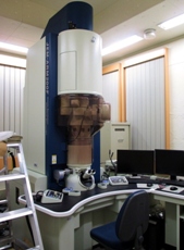 | 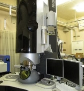 | 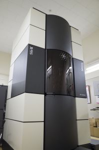 |
| Equipment | Atomic resolution/analytical transmission electron microscope (JEOL/JEM-ARM200F) | Sub Angstrom Resolution analytical transmission electron microscope (FEI-Company/ Titan80-300) | Ultra high resolution analytical transmission electron microscope (Titan³ 60-300 Probe Corrector) |
| Features | Equipped with Cold-FE electron gun Acceleration voltage: 200kV/80kV Irradiation system and imaging system equipped with spherical aberration correction device [Double collector] Ultra-high resolution TEM STEM observation EDS and EELS analysis | Acceleration voltage: 300kV/80kV With spherical aberration correction device High resolution TEM STEM observation EDS analysis EELS analysis 3D analysis | FE electron gun (X-FEG) (Acceleration voltage: 60kV, 300kV) TEM resolution: 130pm STEM high resolution; 70pm 2k x 2k CCD camera super X EDS system (coronal SDD type) |
| List No. | 4 | 5 |
|---|---|---|
| Image | | 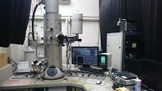 |
| Name | Ultra-high resolution analytical electron microscope (Titan³ 60-300 Double Corrector) | Analytical electron microscope (Topcon EM-002B) |
| Features | FE electron gun (X-FEG) (Acceleration voltage: 60kV, 300kV) TEM resolution:80pm, 70pm STEM resolution; 70pm Energy resolution; 0.85eV,0.3eV 2k x 2k CCD camera super X EDS system (coronal SDD type) | Acceleration voltage:200kV LaB6 electron gun EDS point analysis Precession electron diffraction |
| List No. | 6 | 17 |
|---|---|---|
| Image | 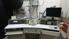 | 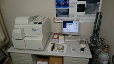 |
| Name | Transmission electron microscope (JEOL JEM-2000EXⅡ) | Thin film cross-section sample preparation device (JEOL EM-09100IS) |
| Features | Accelerating voltage: 200kV LaB6Electron gun High tilt observation (Sample tilt angle: X=±60°, Y=±38°) Sample heating holder (Maximum heating temperature: approx. 800℃) Sample cooling holder | Ion acceleration voltage: 1kV-8kV |
| List No. | 8 / 9 | 10 | 10 |
|---|---|---|---|
| Image | 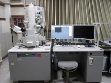 | 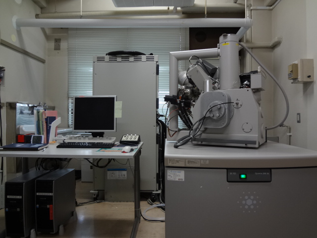 | 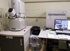 |
| Name | High resolution, low acceleration voltage scanning electron microscope (Hitachi High-Tech/SU8000 /S-5500) | FIB focused ion beam processing equipment (FEI-Company/Quanta 3D) | FIB focused ion beam processing equipment (FEI-Company/Versa 3D) |
| Features | Acceleration voltage: 30kV-0.1kV Low acceleration voltage observation to suppress sample damage STEM mode Stereo photography with charge-up reduction device EDS mapping analysis | SEM/SIM observation Dual beam FIB SEM acceleration voltage: 30kV Sample pickup: Omniprobe | FE electron gun equipped SEM/SIM observation Dual beam FIB SEM (SE/DSE/SIM) acceleration voltage: 30kV Sample pickup: EasyLift 3D construction Slice & View |
| List No. | 19 | 20 |
|---|---|---|
| Image | 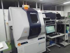 | 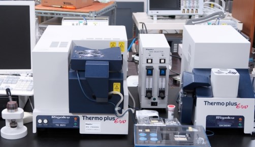 |
| Name | High output fully automatic horizontal multipurpose X-ray diffraction device | Thermal analysis device |
| Features | Made by Rigaku Corporation Model: SmartLab 9SW Output: 9kW ●Using a high-intensity Cu radiation source, it is possible to quickly measure powder, thin film samples, etc. ●We can meet a variety of needs, such as in-plane measurement and variable temperature measurement using a DSC unit. | Specifications: TG-DTA temperature range; room temperature to 1100 ℃ (normal use 1000 ℃) TG-DTA maximum measurement sample amount; 1 g ・TG-DTA maximum heating rate; 100 ℃/min ・DSC temperature range; room temperature to 725 ℃ ・DSC maximum range; ±100 mW ● It is equipped with a differential thermal balance (TG-DTA) TG8120 and a differential scanning calorimeter (DSC) DSC8230. ● Simultaneous measurement device for TG and DTA is possible. DSC is a method that measures the amount of heat absorbed and absorbed by a sample when its temperature is scanned. |
Introduction of main support equipment (Affiliation: Research Center for Macromolecule Analysis, Graduate School of Science)
| List No. | 21 | 28 |
|---|---|---|
| Image | 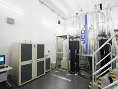 | 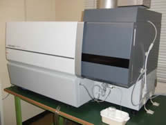 |
| Name | Nuclear magnetic resonance apparatus | ICP emission spectrometer |
| Characteristics | Made by JEOL Ltd. Model: 800MHz NMR JNM-ECA 800 This NMR is equipped with a measuring system with a sample tube outer diameter of 1 mm that can rotate at magic angles at 80 kHz, the world’s fastest speed, and enables ultra-high sensitivity measurements of extremely small amounts of solid (0.8 μL) and solution (0.07 mL) samples. | Made by Shimadzu Corporation Model: ICPE-9000 ●Has a high detection capability of ppb level and a wide analysis concentration range of 5 to 6 orders of magnitude, allowing simultaneous analysis of multiple elements. ●The amount of interference of coexisting elements can be accurately evaluated, all elements can be calibrated at once, and it is equipped with an automatic wavelength selection system that is ideal for analysis. |
This page was created by an AI agent.